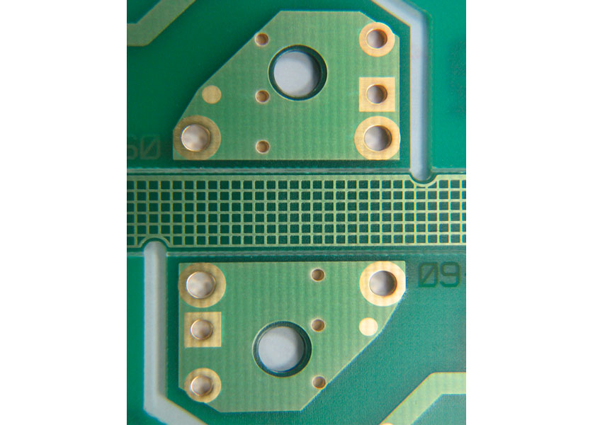
PASSIVATED COPPER
ORGANIC SOLDER PRESERVATIVE (OSP)
The passivation finishing of the uncovered copper on the printed circuit board is a chemical treatment used to prevent oxidation. The thickness of the protective film that is deposited on the copper is between 0.1 and 0.4 μm (microns); this film allows the board weldability for at least one year if the product is stored in its original packages at room temperature (10-30°C) and protected from light. The PCBs that are processed through this chemical approach are subjected to a maximum temperature of 42°C and a final drying with hot air at 70°C.
LEAD FREE TINNING
HOT AIR SOLDER LEVEL (H.A.S.L.)
The process consists of dipping the PCBs in a well with melted tin (lead-free). When they emerge, the tin in excess is removed from the holes and from the PADs using blades with hot air jet under pressure acting as "leveler", leaving a thickness of about 2-3 μm; this thickness often depends on the printed circuit board layout. H.A.S.L.'s limitation is the flatness of the deposited tin; even with the best technology, it is not possible to create footprints for SMD components such as "fine pitch" and BGA (Ball Grid Array).
LEAD FREE TINNING
SELECTIVE CHEMICAL TINE LINE
The PCBs are processed before the packaging stage, in a horizontal line with chemical baths where the pure tin, "lead-free", is deposited exclusively on the uncovered copper areas previously treated (cleaned). The material, during the entire process is subjected to a maximum temperature of 63°C in the bath of Chemical Tin and 75°C in the hot air furnace for final drying. The process introduced to meet the European RoHS directives, allows depositing a thickness of tin alloy ranging from 0.95 to 1.14 μm, perfectly flat and uniform. In addition, if the process is continuously controlled, it is possible to ensure a storage of one year and 2/3 cycles or reflow (inter-metallic melting process during welding of electronic components). The process with selective chemical tin will be used in the future; it will replace over time the H.A.S.L. because, thanks to its perfect flatness, all SMD components such as BGA, "fine pitch" and "small chips" are easily weldable on both circuit sides (Top and bottom sides).
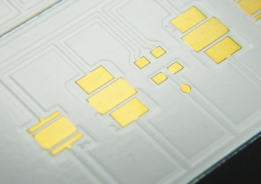
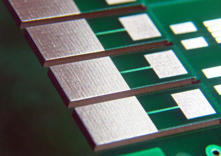
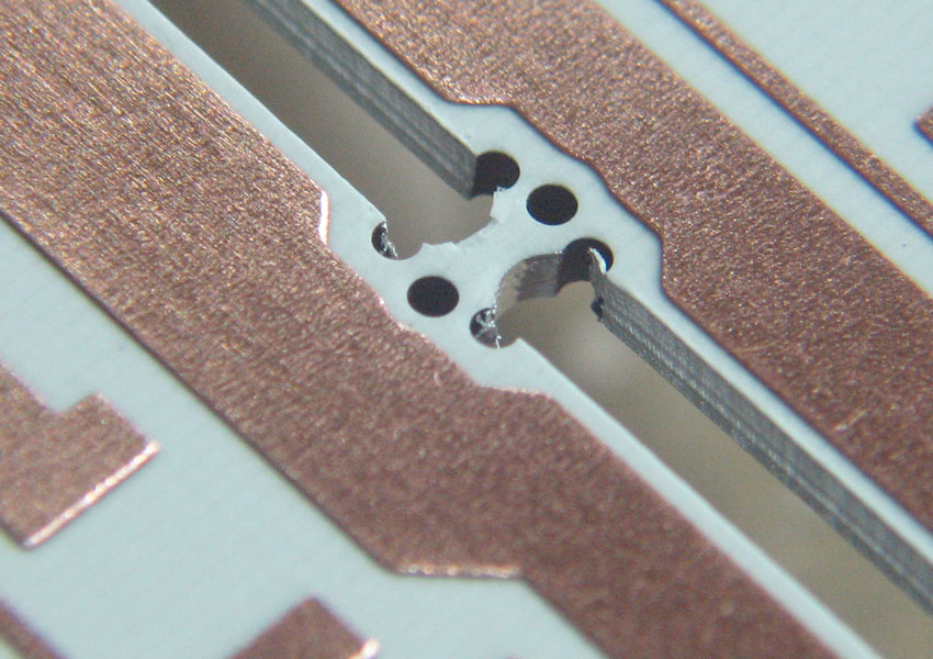
CHEMICAL / ELECTROLYTIC GOLD
SELECTIVE GOLD-PLATING
It is the best and the most expensive finish that can be applied on PCBs, especially to those with high technological content, such as BGA, "fine pitch" and "sliding contacts". This process complies with the IPC-4552 directive; the process requires first a deposit of nickel with an average thickness of 5 μm, (only on copper PADs, cleaned with the previous chemical process), then as a last step a deposit of pure gold, with an average thickness of 0.05 μm; the last step constitutes a finishing very resistant to multiple remelting passages and contact movements. PCBs with gold finishing may be stored for a period longer than one year.
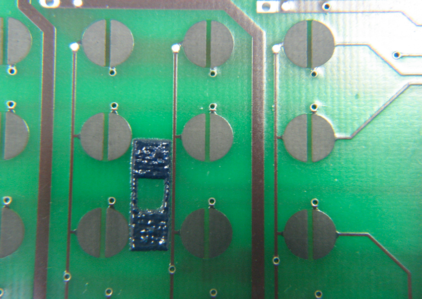
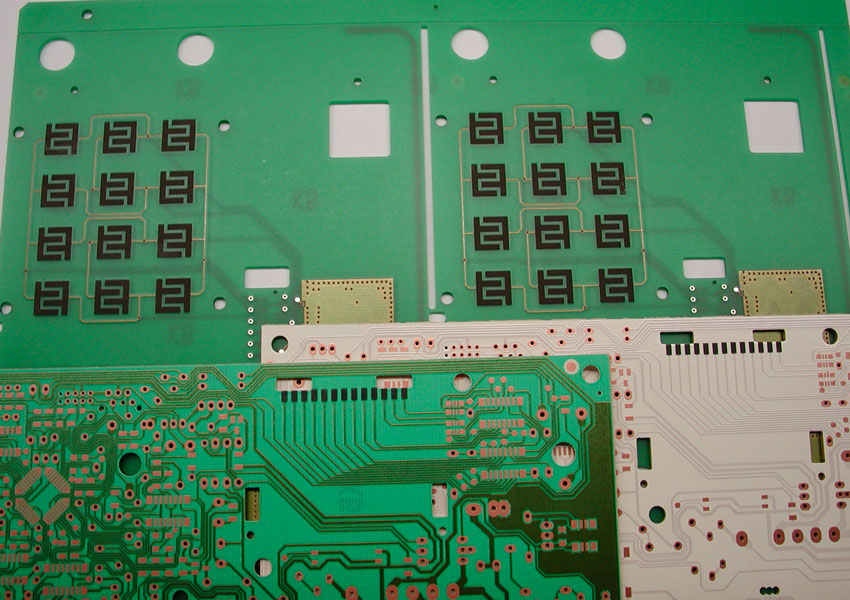
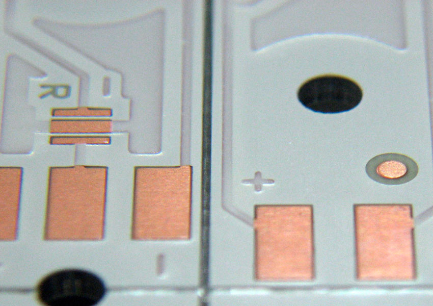
GRAPHITE
SILKSCREEN PRINTING
This process use an ink containing carbon that is generally applied on the copper PADs and acting as sliding contacts for knobs, membranes, LCD, etc. on customer's request. This carbon ink is applied and processed by special plants for silkscreen printing. Its characteristic is to be a conductive element with a "Resistance" <1 Ω (normally between 0.2 and 0.5 Ω). In addition, high precision is necessary in overlapping the concerned PADs.