

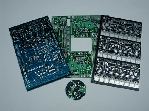
P.A.C. experience and technology lead the company to offer design support and manufacturing of printed circuit boards on custom orders, covering almost all sectors that require the use of electronics.
Obviously we use the classical techniques to assemble the components on the circuit board, known with the following two acronyms: THT (Through Hole Technology) and SMT (Surface Mount Technology).
Through hole technology means the assembly of components whose terminals (leads), properly bent, go through the holes previously drilled on the pcb, and then welded on a copper pad. The pcb side where the various components are mounted is called "Component Side (L.C)", while the other side where the leads are welded on the pads and the tracks are located is called "Solder Side (L.S.)".
Differently, the surface mount technique (SMT) uses components called SMD (Surface Mount Device). With this technique, the component leads do not pass through the hole, but they are welded on the component side; therefore, the "component side, L.C." coincides with the "solder side, L.S.".
If the tracks on the pcb are located on a single side, the pcb is called "single-sided". This type of printed circuit board is mainly used for civil use such as for boilers, electrical appliances, emergency lamps, automatic gates, etc.
If the two sides are used, the pcb is called "double-sided" and its main application is for professional use in the automotive, electro-medical, telecommunications, etc.
The three printed circuit types described above may also differ for finishing, coloring of the protective paint and type of material used as support (FR2, FR4, or CEM1 CEM3-T and Metal-Core).
P.A.C. is also experienced in the production of printed circuit boards on new metal substrates such as aluminum and copper, essential for optimum thermal conductivity, thus allowing extremely easy machining and assembly of the various power components.
The use of these metal substrates is combined with the use of IMS technology (Insulated Metal Substrate) that is an insulated metal support characterized by three main elements:
1) a heat dissipative metal base;
2) a dielectric insulator;
3) a conductive copper layer.
The printed circuit boards made with IMS technology are also named with the initials "Metal Core, MCPCB"; they are suitable for applications requiring significant electric currents such as the following: Industrial sectors: power supplies, inverters, welding machines; lighting sectors:
High power LED, lighting technology, headlights, street lamps; Automotive: voltage regulator, ignition systems, control units, fans.
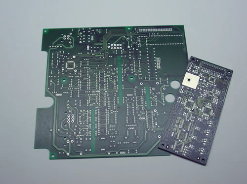
In order to reduce the PCB dimensions as much as possible, components can be arranged on different interconnection levels by using both the Through hole and Surface mount technologies. In this way it is possible to cross over different tracks placed on different layers; this type of printed circuit board is called as "multi-layer", because different interconnection levels are made on the same board. This multi-layer PCB is mainly used for sophisticated equipment such as PC motherboards, mobile phones, military and aerospace equipment.
The manufacturing of a multilayer PCB requires sophisticated equipment used only at industrial level.
P.A.C. can also apply, on printed circuit boards, protective materials such as graphite, used to improve the electrical contact of keys, display etc., or "SPELLICOLABILE" a paint peel stripping product (solder-mask) designed to prevent welding on particular areas to be worked on later.
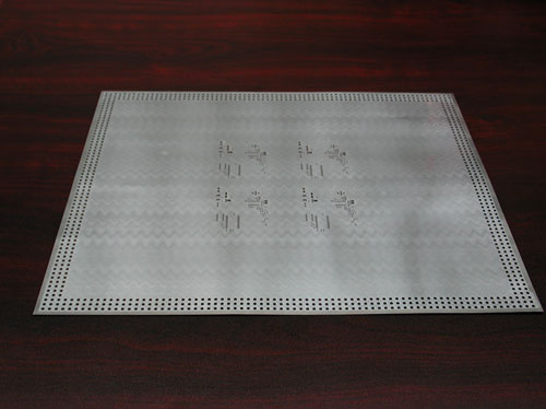
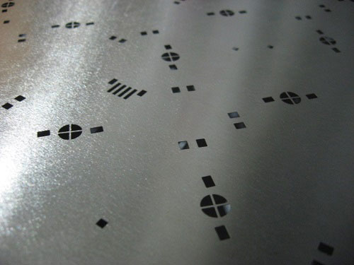
The "SMT metal sheets" are made by P.A.C. for international customers using the "photo-etching" method that unlike the mechanical drilling is fast and does not produce metal burr.
Advantageous both for the manufacturing of prototypes and production series as well as for precision-based applications using also very thin thicknesses such as 0.100 – 0.150 – 0.200 mm.