

SECTORS
The specific know-how that P.A.C. has acquired to date allows it to be a valid partner for industrial clients with high technological applications, such as in the medical, automation, rail, marine, telecommunications, earth moving machines and oil sectors.
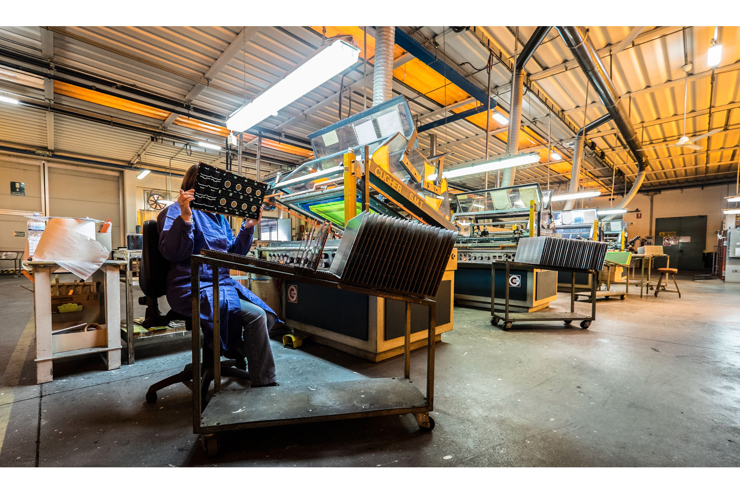
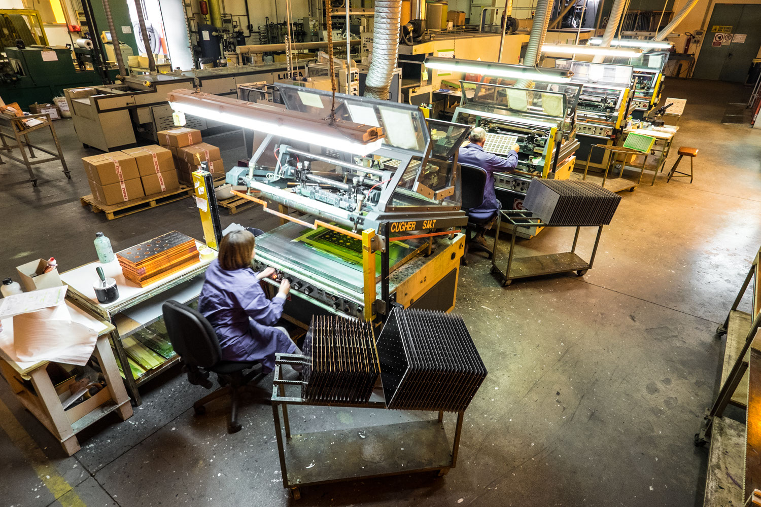
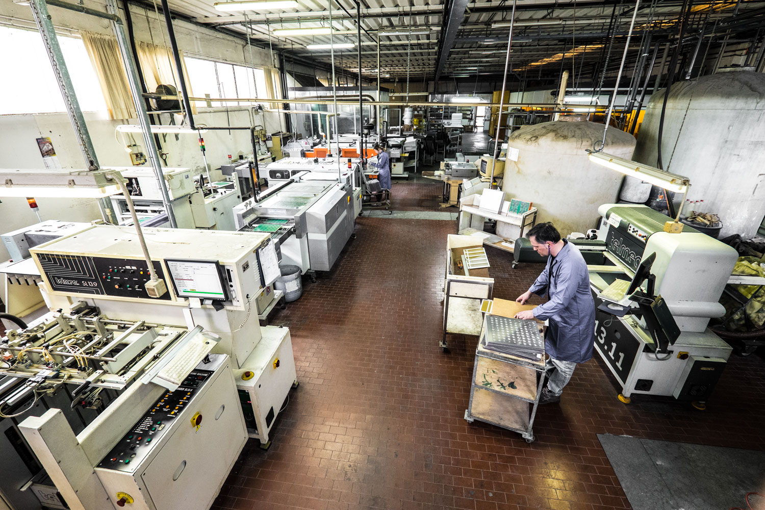
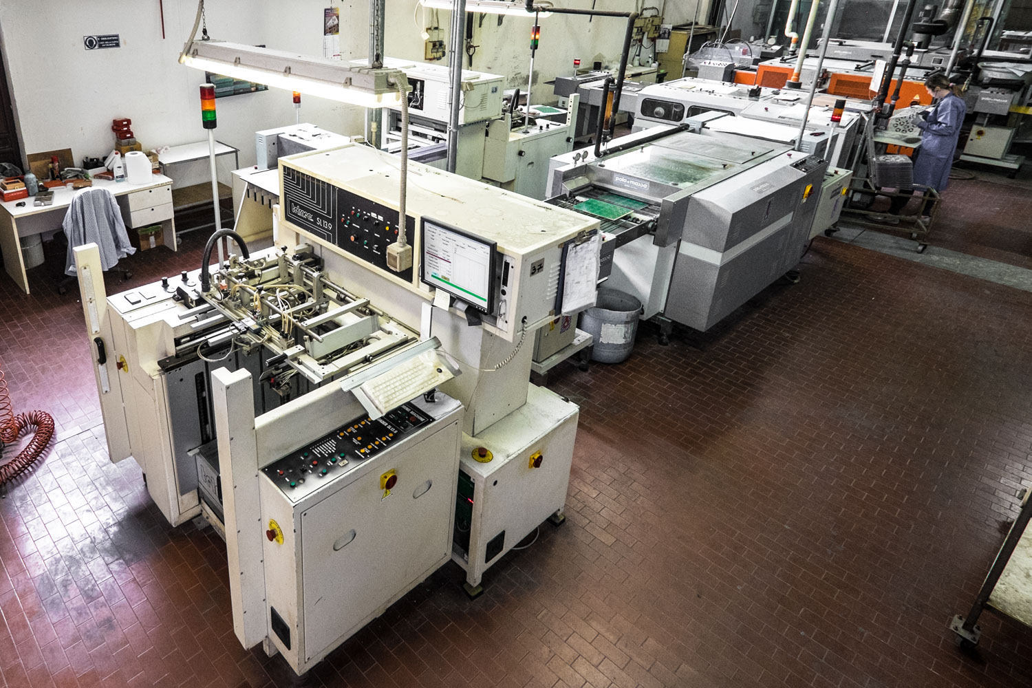
The production of printed circuit boards consists of several processing stages that differ according to the type and finish required; however, the production process can be summarized in the following main stages:
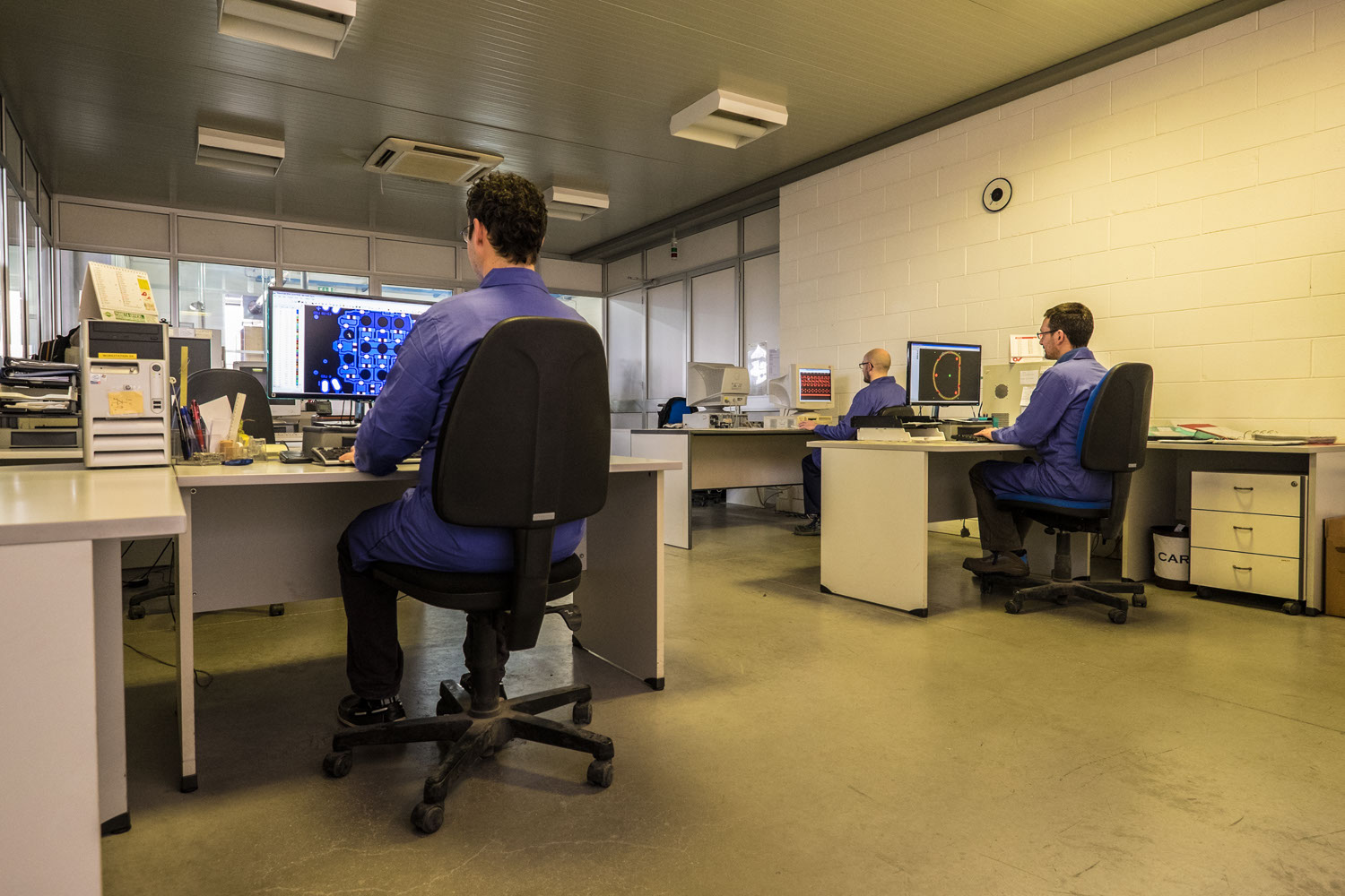
CAD DESIGN
It sets the entire production cycle of the printed circuit board, starting from an accurate check of the customer drawing up to the implementation of all the necessary equipment to produce the printed circuit board.
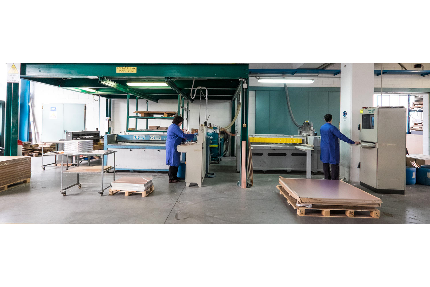
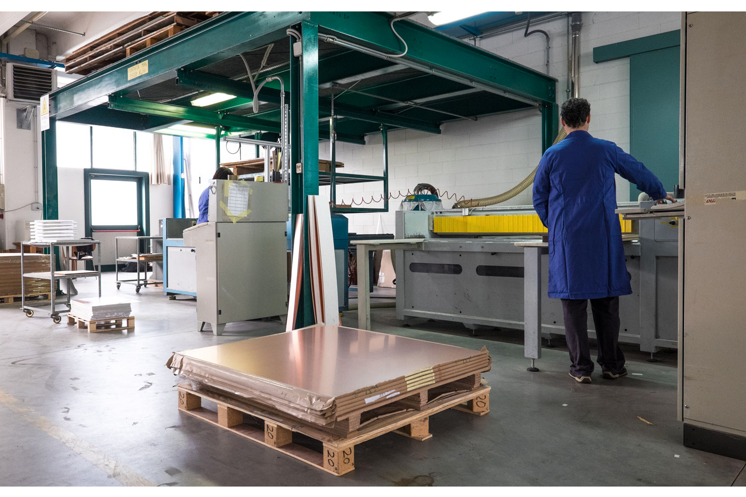
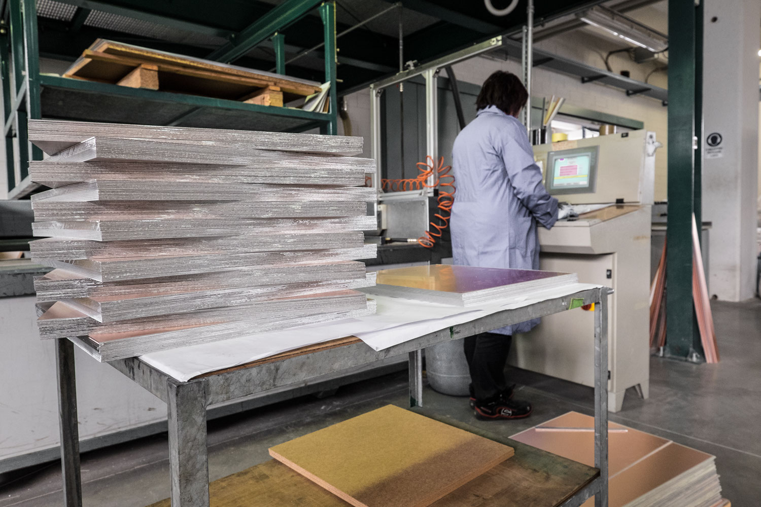
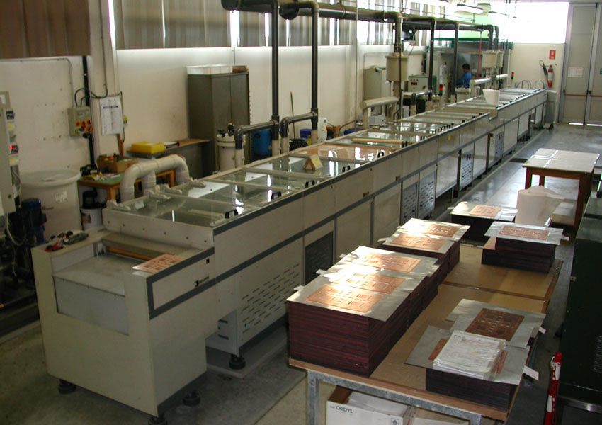
LAMINATE CUTTING
In this department, the various sheets of laminate (raw material) are cut in adequate size panels for the production of the printed circuit boards. Different types of materials are available ranging from 0.2 to 4.0 mm in thickness, with related copper thicknesses ranging from 17, 35, 70, 105, to 400 microns.
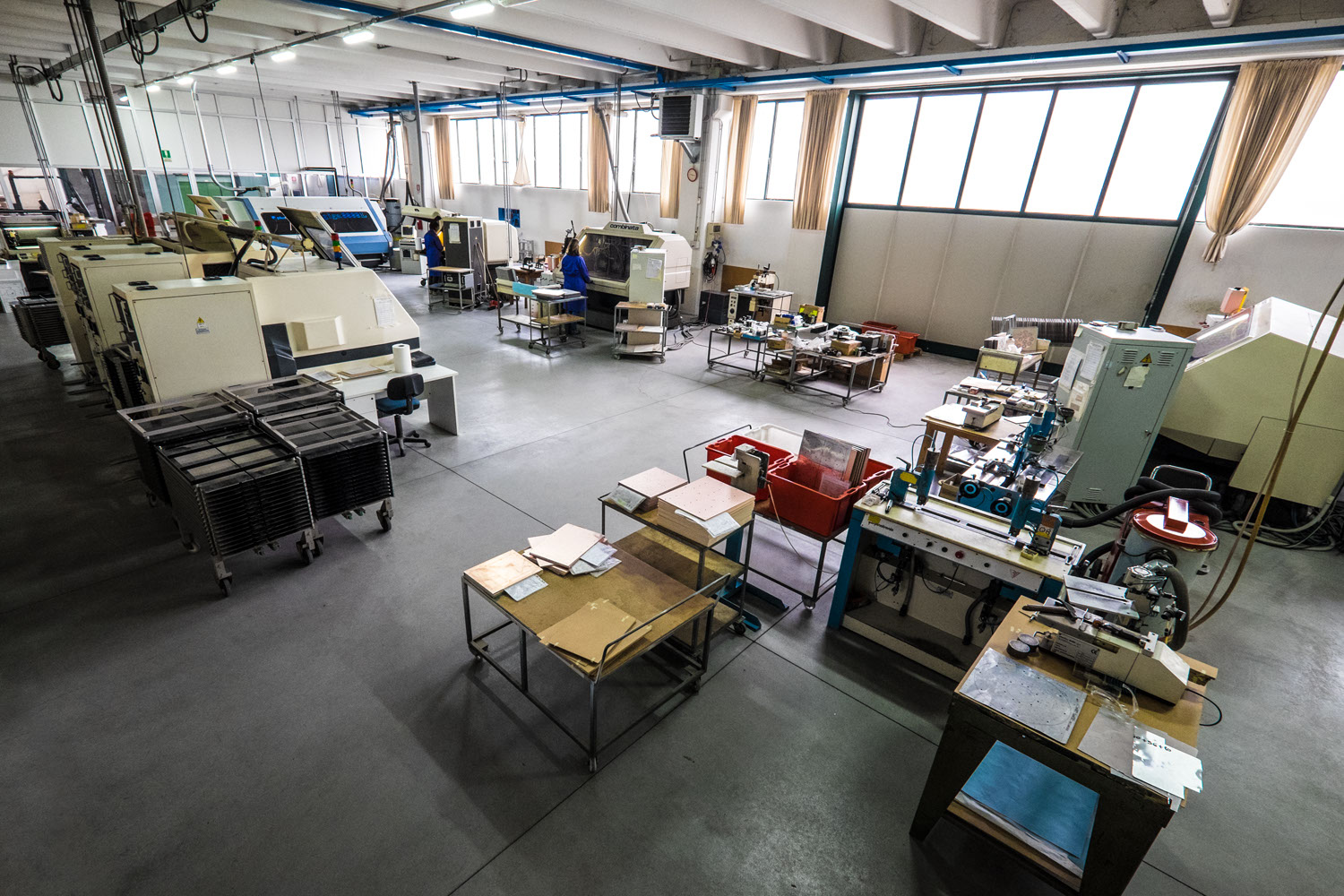
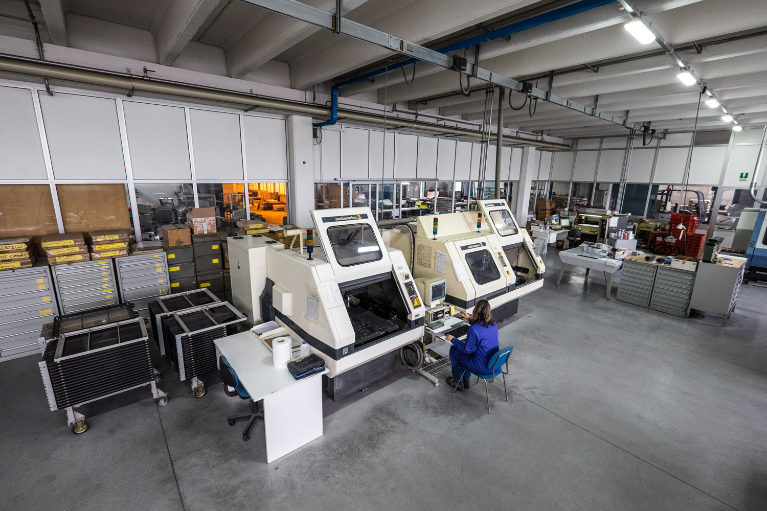
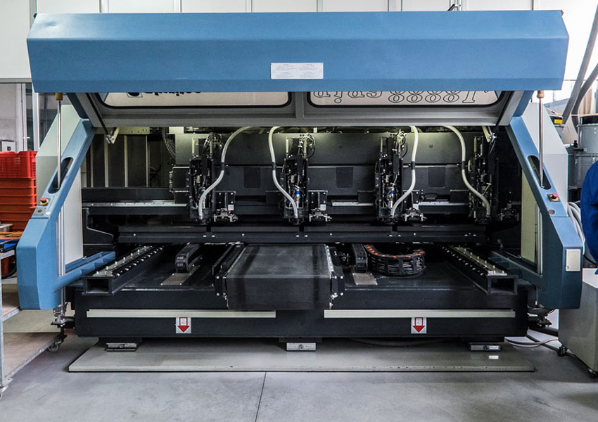
DRILLING
It is carried out using different CNC machines, which guarantee maximum hole precision. We have the latest technology on the market by making available for the customer the highest productivity thanks to the GIGA 8888L drilling machine with 8 heads that allows us to drill and mill in a short time very large batches of printed circuits.
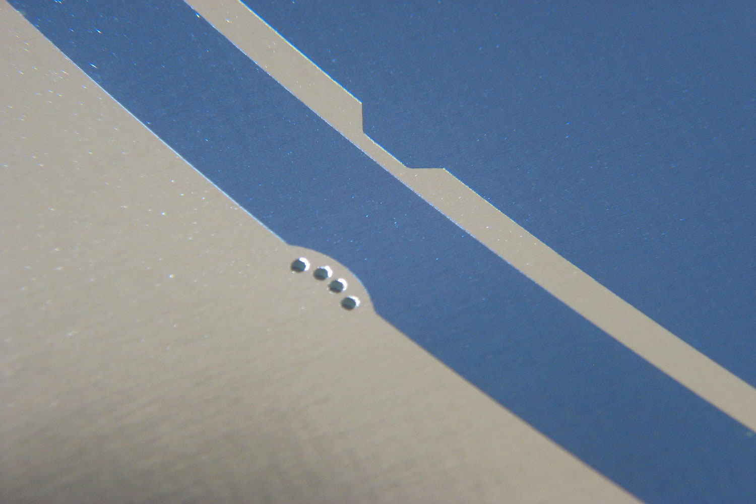
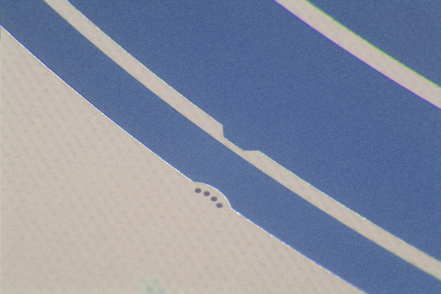
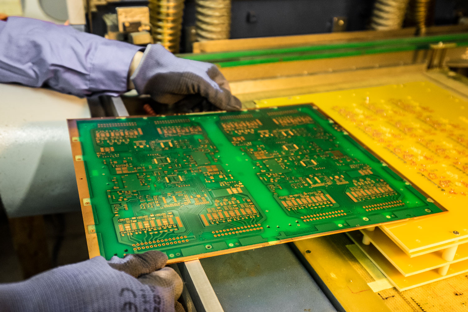
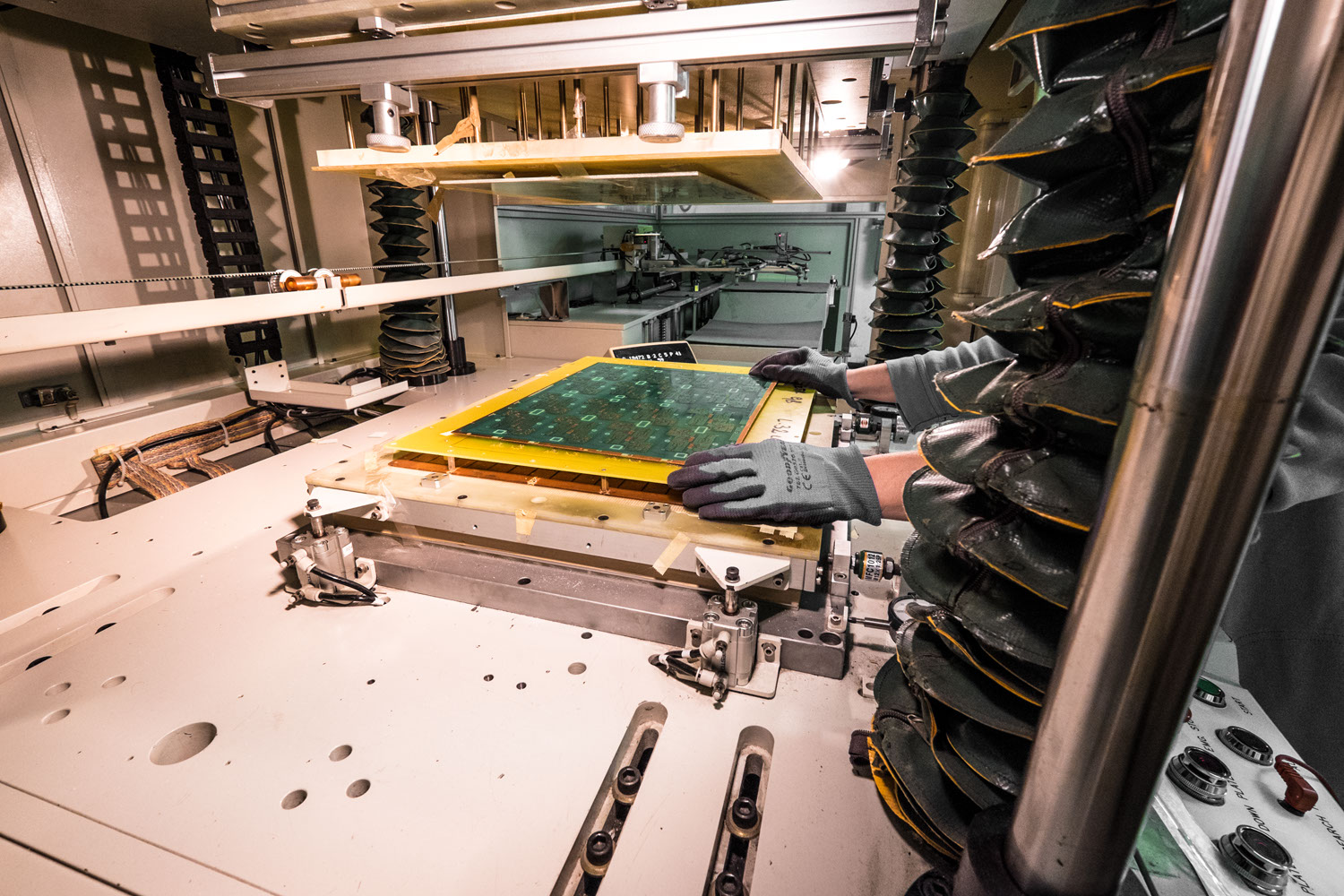
YELLOW ROOM
The image of the printed circuit board on the panels and subsequently also the correct image of the solder resist are obtained in this department through a photographic process.
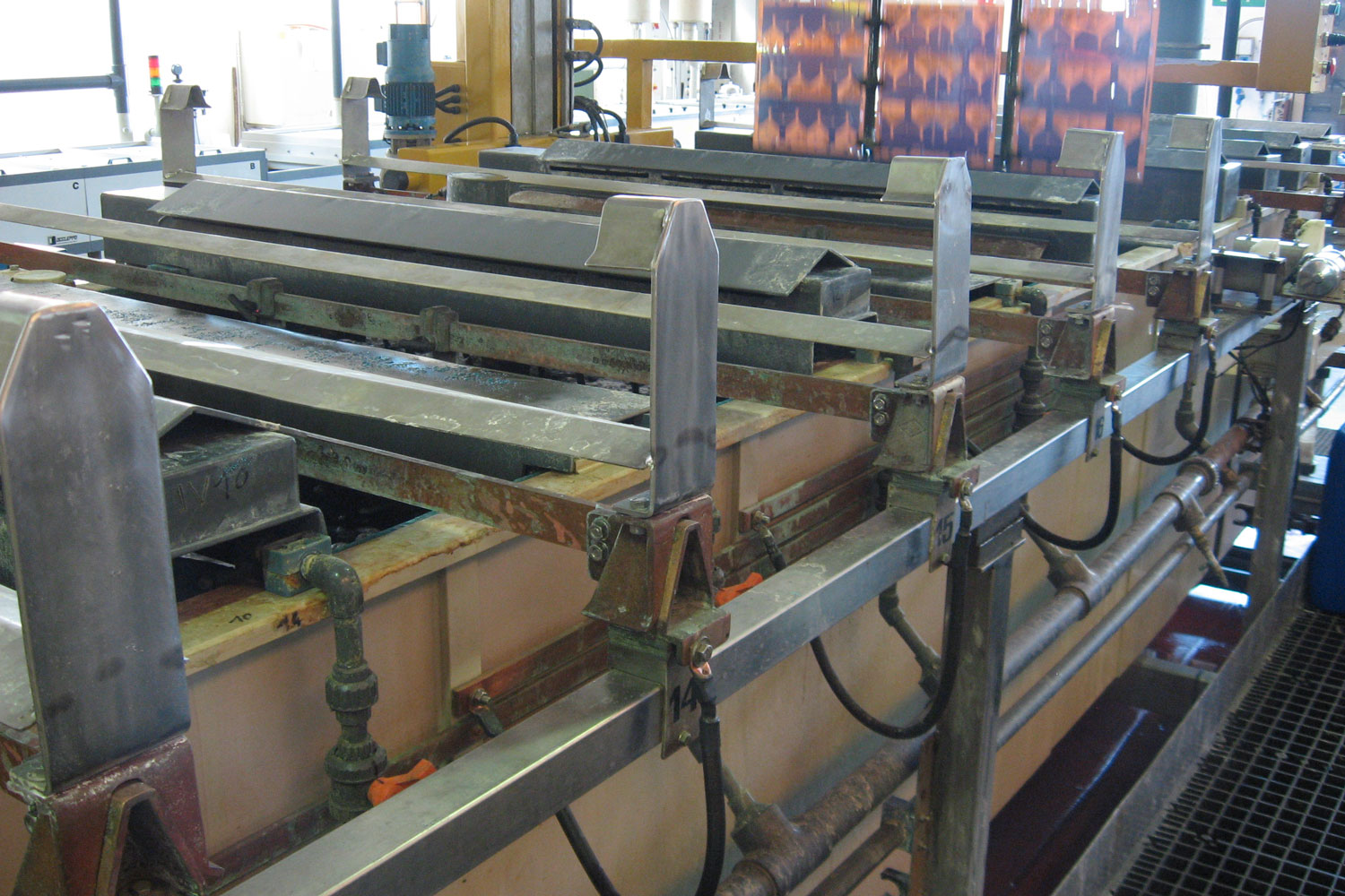
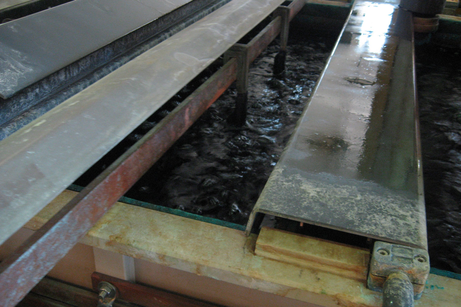
STRIPPING -ENGRAVING
These processes allow the photographic materials to be removed, (previously used to protect the copper part which is not necessary to the circuit diagram) together with the excess copper, thus obtaining tracks and pads as required.
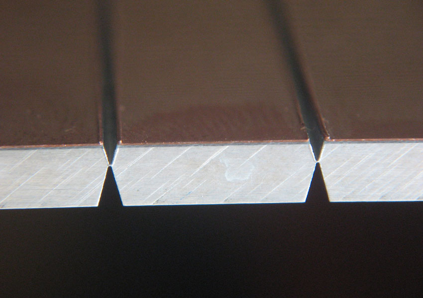
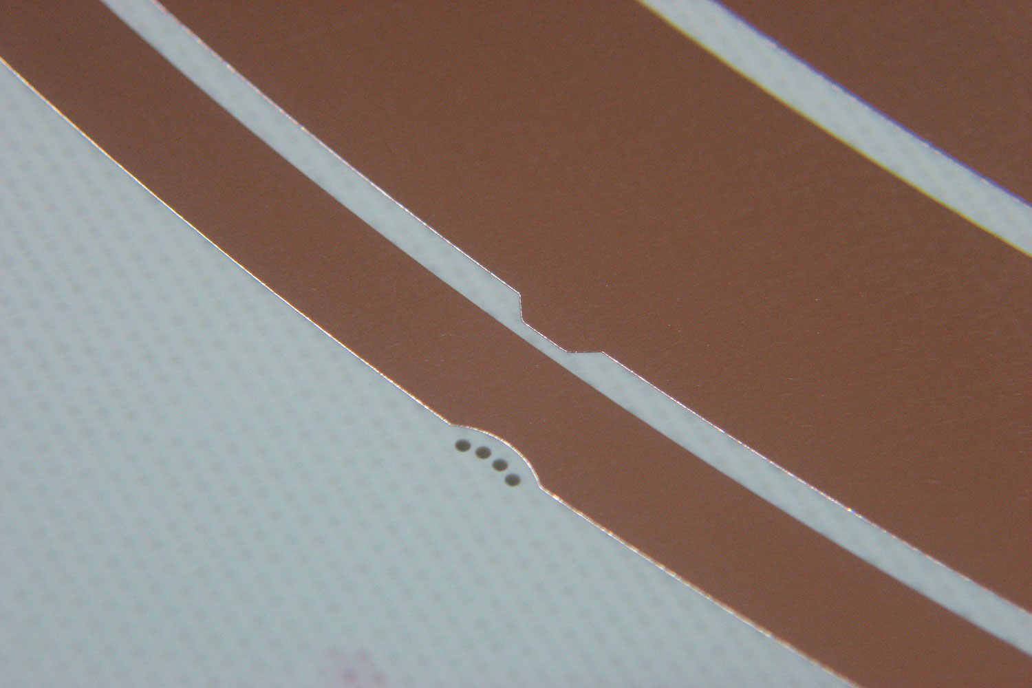
V-SCORING
A "V" shaped separation grooving is carried out on the whole printed circuit, by using precision "widia" or diamond discs; then the CNC machines pre-cut the boards, on both surfaces, thus allowing, after component assembly, the separation of the whole printed circuit board into individual elements.
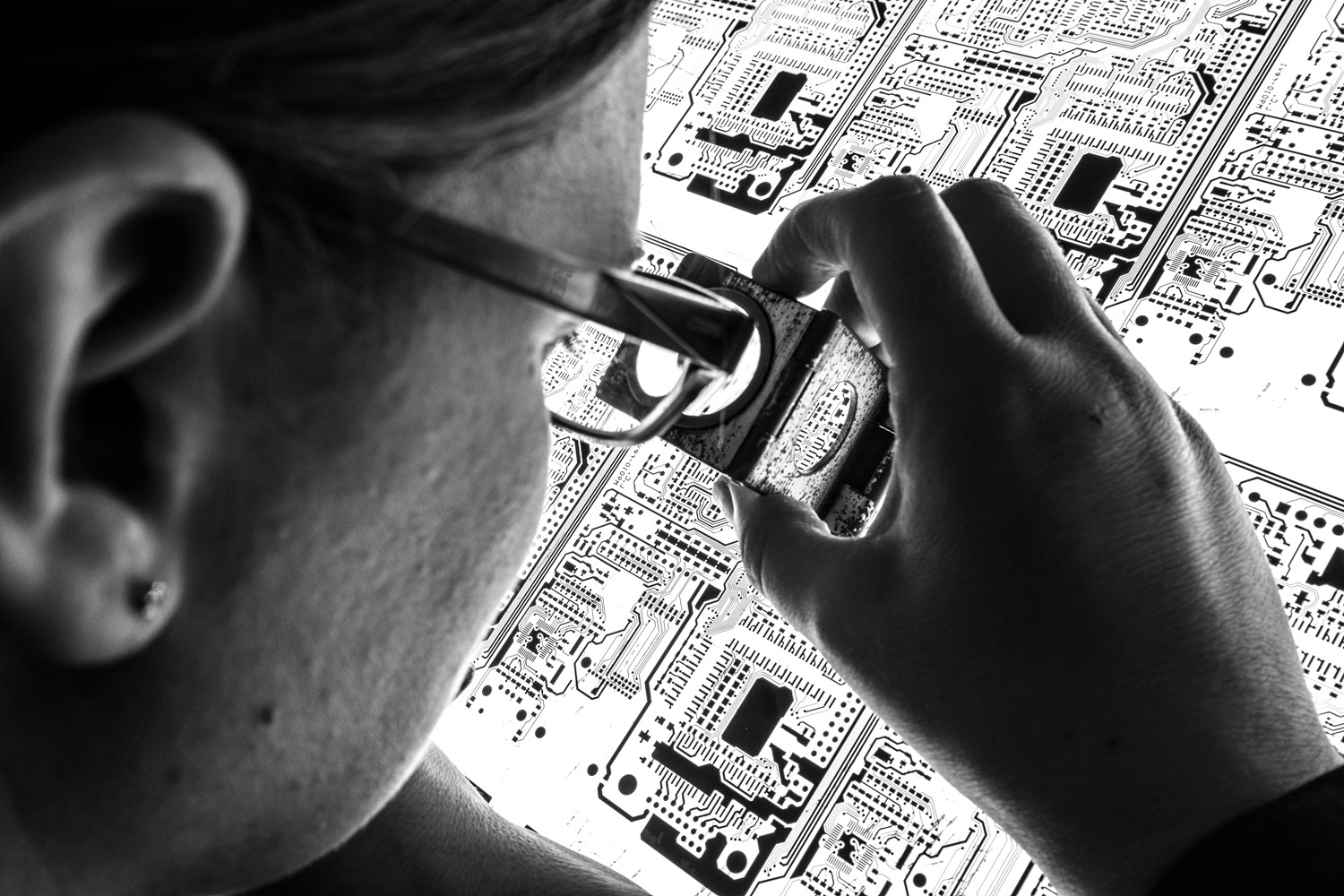
ELECTRICAL TEST
A functional check on 100% of the production batch is carried out by using special machines, including a "PRECISE Machine" which performs a double tests on the PCB. This process, together with all the other checks carried out during the production cycle, allows us to deliver to our customers a HIGH QUALITY product.
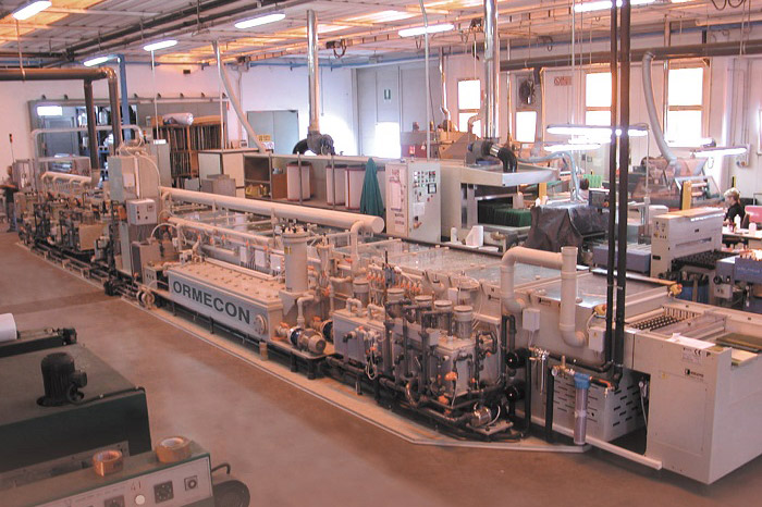
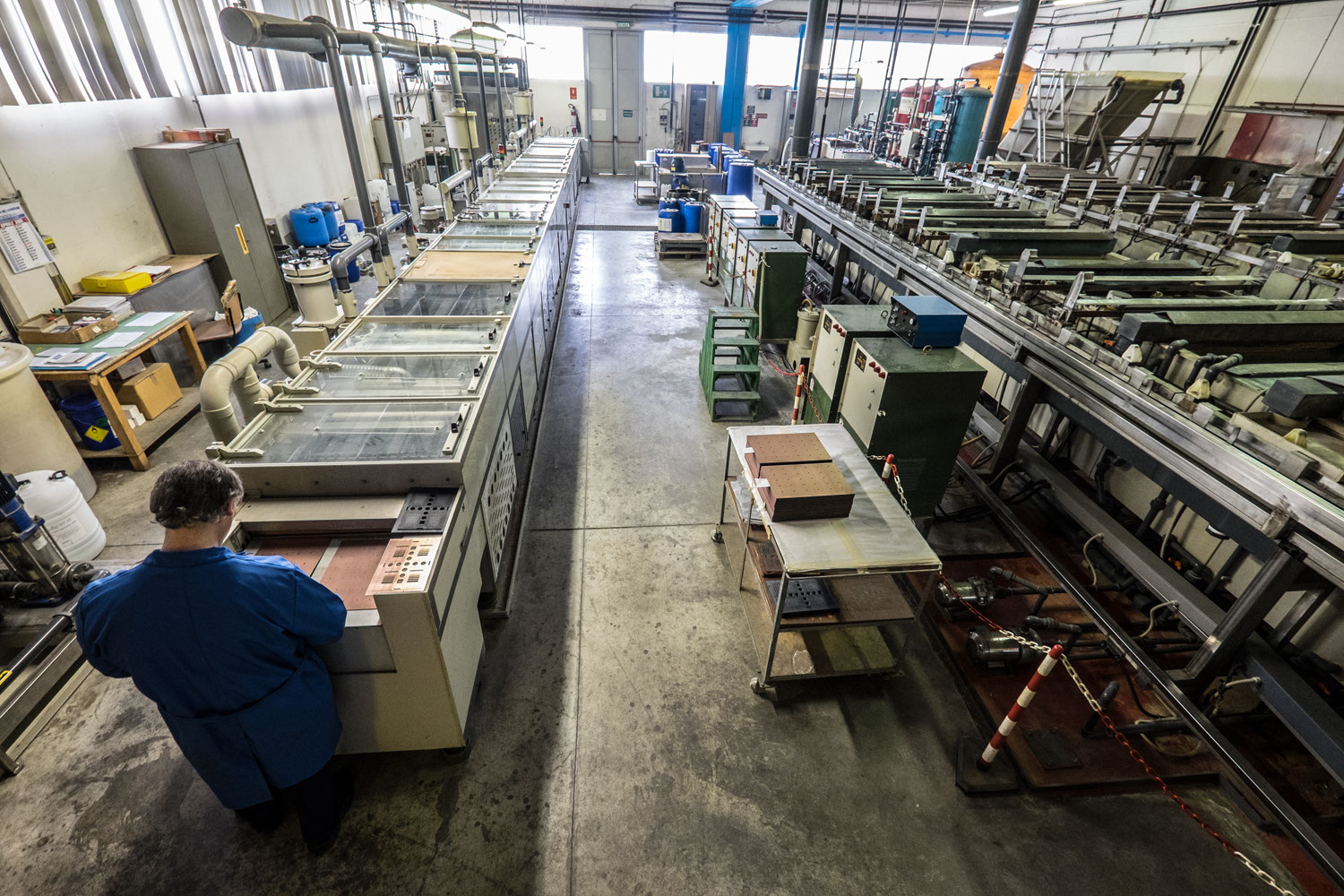
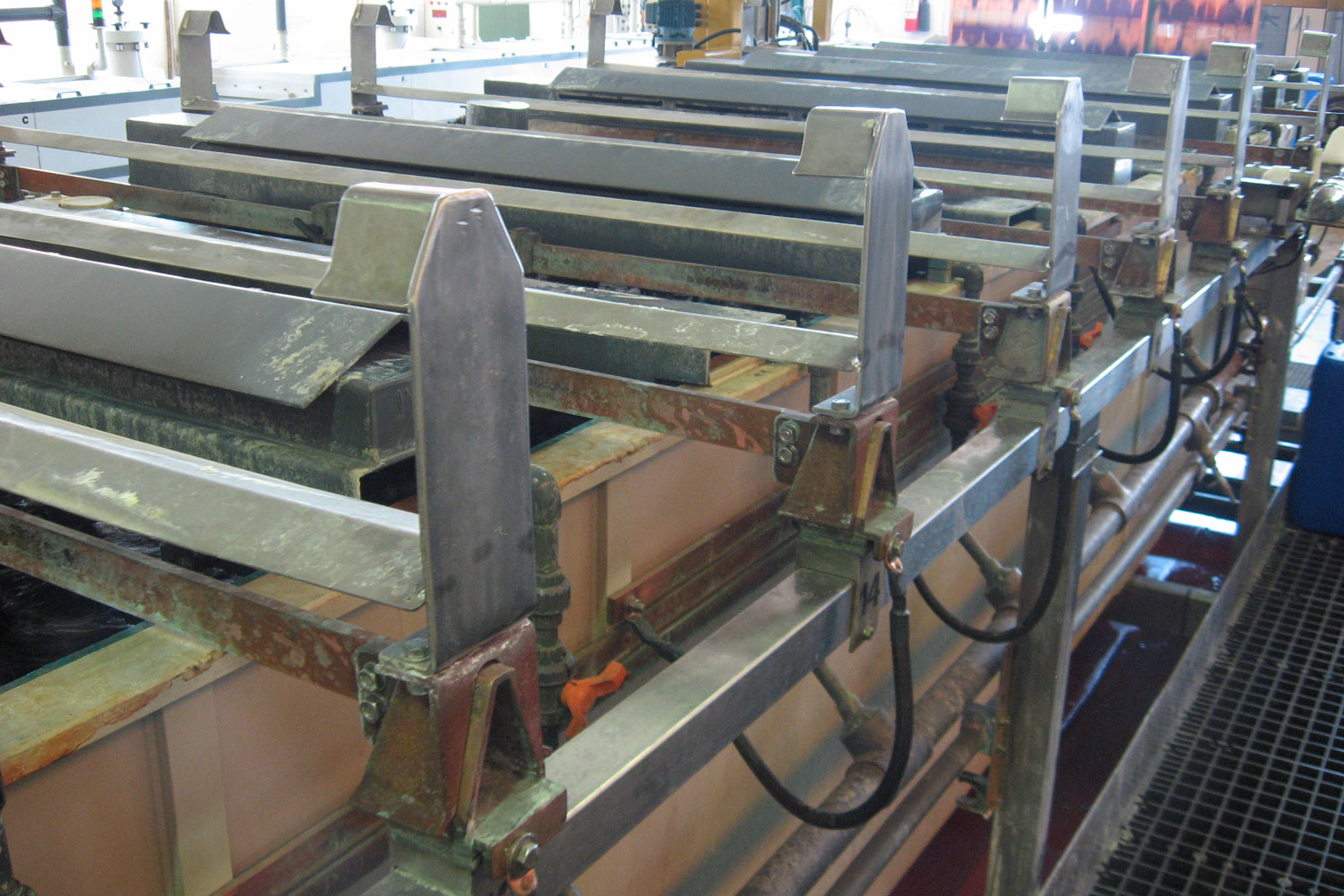
CHEMICAL TIN LINE
Manufacturing process for the production of "lead-free PCBs". It consists in a selective chemical tinning, perfectly planar and highly weldable that allows to deposit, only on the welding pad, a compact and crystalline layer of pure tin, thanks to a particular product organometallic, which is interposed between the copper and tin, slowing the formation of intermetallic compounds.